This application note provides tables of suitable hkil reflections for the measurement of GaN wafers with the most common semi-polar and non-polar orientations. For completion the 0001 polar orientation is also included.
Gallium nitride and its alloys continue to play an important role worldwide in the optoelectronics industry and in particular in the production of light emitting diodes (LEDs). In the drive for higher efficiencies and novel device design there is increasing interest in the growth of GaN thin films with exotic orientations. High-resolution XRD analyses are employed extensively in the fabrication of GaN layer structures for devices. Typically peak FWHM (full width half maximum) of MQW (multiple quantum well) Bragg peaks are measured for quality control of wafers.
Gallium nitride and its alloys continue to play an important role worldwide in the optoelectronics industry and in particular in the production of light emitting diodes (LEDs). In the drive for higher efficiencies and novel device design there is increasing interest in the growth of GaN thin films with exotic orientations. High-resolution XRD analyses are employed extensively in the fabrication of GaN layer structures for devices. Typically peak FWHM (full width half maximum) of MQW (multiple quantum well) Bragg peaks are measured for quality control of wafers.
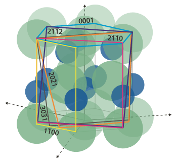
A challenge for diffractionists working with exotic orientations is to find appropriate hkil reflections for the measurement of Bragg peak widths and positions. Figure 1 illustrates the most common crystallographic layer orientations with reference to the hexagonal GaN unit cell. The first GaN devices were fabricated with (0001) oriented ’polar‘ layers. Subsequently ‘non-polar’ layers have been employed. These typically have orientations (2110) or (1100). ‘Semi- polar’ layers have orientations intermediate between those of polar and non-polar layers. The most common semi-polar layers are (2112), (2021) and (3031) [For further information about the hkil notation see references 1 and 2
The polar structure of GaN gives rise to strong piezoelectric and spontaneous polarization fields in the [0001] direction. Research has shown that the efficiency of GaN-based optoelectronic devices can be improved by growing layers with non-polar or semi-polar orientations. The orientations that are most favorable depend upon a collection of factors such as growth method, substrate types and device structure. The design and growth of non-polar and semi-polar devices is an active research area in today’s GaN industries.
This application note provides tables of suitable hkil reflections for the measurement of GaN wafers with the most common semi-polar and non-polar orientations. For completion the 0001 polar orientation is also included.
Figure 1. Schematic illustration of the GaN unit cell showing the six most common layer orientations used in GaN technologies
When considering which Bragg hkil reflections are suitable for analysis using high-resolution XRD, we must consider the crystal structure, wafer orientation and the geometric limitations of the measurement. The crystal structure determines which hkil reflections exist and their relative intensities. The wafer orientation determines the necessary angle of incidence, omega (ω), for the reflection. The X-ray wavelength, λ, and the hkil plane spacing dhkil dictate the 2theta (2θ) angle, given by λ = 2dsinθ. The instrument and the measurement method determine the geometrical limits. Typically the maximum 2θ measurement is around 160°. For coplanar reflection omega is constrained by the condition 2θ > ω > 0. The principal components to consider for each of the coplanar and in-plane geometries are shown in Figures 2 and 3 respectively. Each reflection from a single set of planes with index hkil can be represented by a single hkil reciprocal lattice spot. The diagrams show how the spots relate to the incident beam angle, ω, the diffracted beam angle, 2θ and the azimuth .
All of the available reflections for a particular wafer orientation and geometry, can be described by a diagram such as Figure 4 showing all of the hkil spots corresponding to the available reflections for an 0001 oriented GaN layer. The reflections that share orthogonal azimuths are highlighted in yellow and blue. The symmetric reflections are shown here in green. The sample wafer is indicated by the large gray disc. The x,y,z axes are linked to key directions in the wafer. The azimuth angle, , refers to the clockwise angular in-plane rotation from the x axis to the azimuth containing the hkil reciprocal lattice spot (see Figure 3).
Figure 2. A schematic illustration showing coplanar scattering geometry for a set of hkil planes. The incident beam is shown by the red arrow, the diffracted beam by the orange arrow. For the scattering condition, these two arrows are represented by vectors with lengths 1/λ, the scattering vector Q has length = 1/dhkil and is normal to the corresponding hkil planes. The plane containing the incident and diffracted beams is called the diffraction plane. In coplanar geometry the surface normal is coincident with the diffraction plane [see reference 2 for a more detailed description].
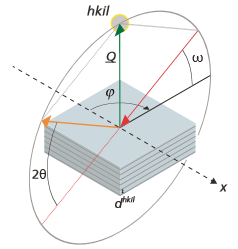
Figure 3. A schematic illustration showing
in-plane scattering geometry for a set of hkil planes. The incident beam is shown by the red arrow, the diffracted beam by the orange arrow. For the scattering condition, these two arrows are represented by vectors with lengths 1/λ, the scattering vector Q has length = 1/dhkil and is normal to the corresponding hkil planes. The plane containing the incident and diffracted beams is called the diffraction plane. For in-plane geometry the surface normal is orthogonal to the diffraction plane [2].
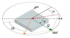
Figure 4. Schematic illustration showing all of the available GaN hkil reflections for the 0001 polar orientation
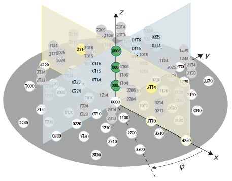
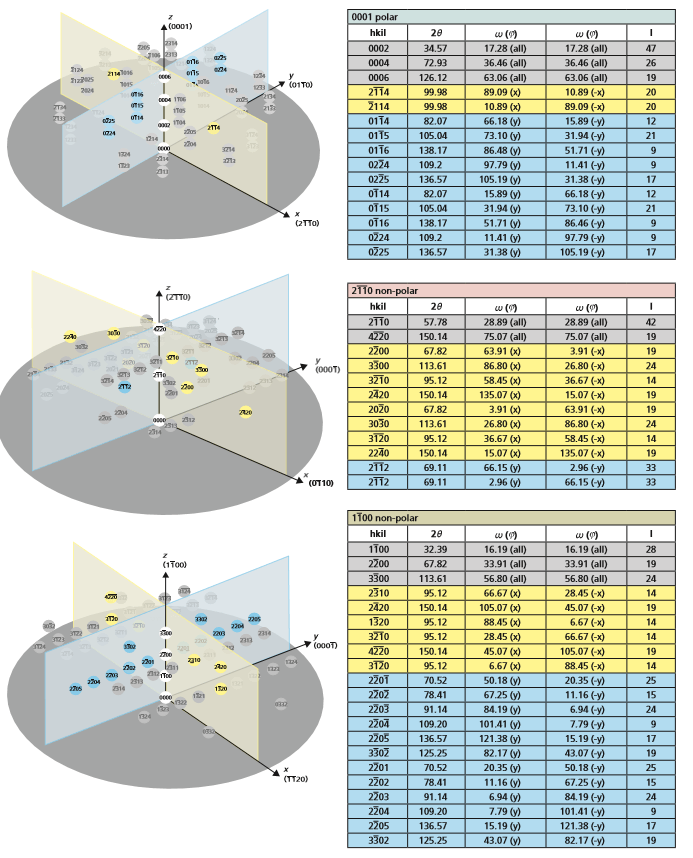
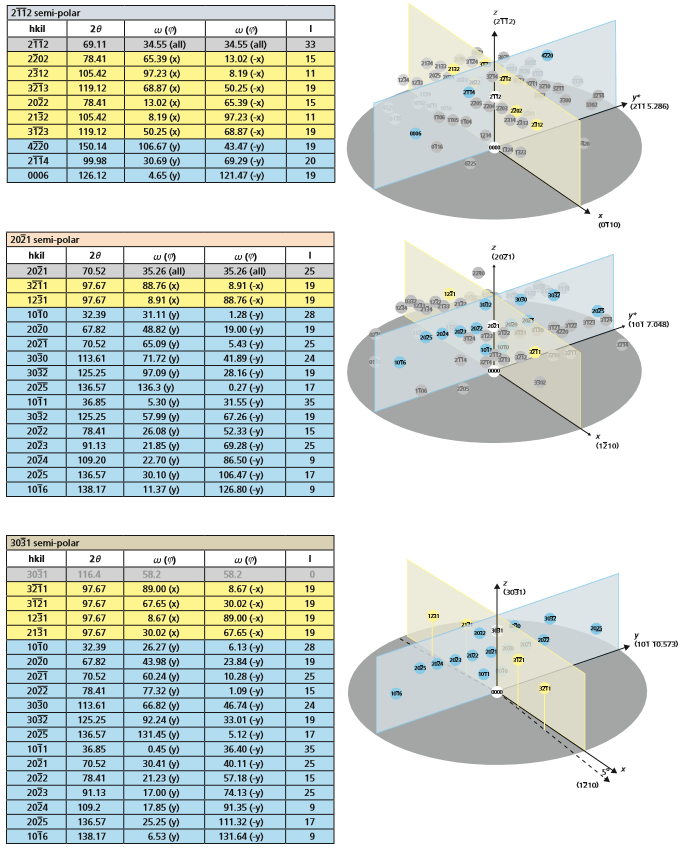
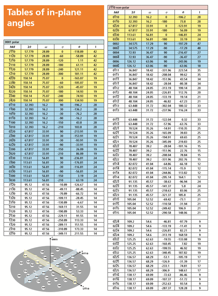
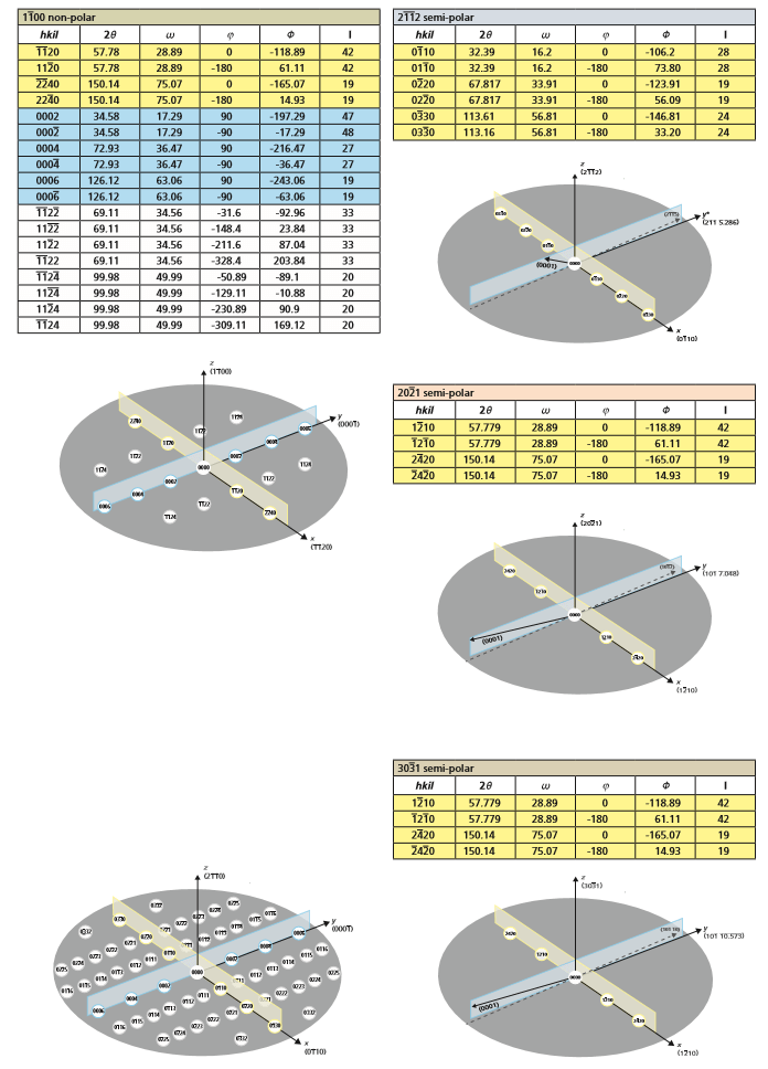
Note that h, k, i and l are positive or negative integers. The format for describing a negative integer can vary between publications, for example minus one can appear as 1, 1 or -1. Every hkil spot can be represented by its 2θ and ω values and the azimuth, , in which it can be found. These values are presented together with estimated relative intensities [3] on pages 4-7, for six of the most common GaN wafer orientations. In order to identify more clearly the useful reflections they are separated into coplanar reflections (on pages 4 and 5) and in-plane reflections (on pages 6 and 7). Only the reflections that show any scattering intensity are considered, with the exception of the 3031 reflection, which has zero intensity but is shown only for illustrative purposes. Note, there is no useful symmetric reflection for the 3031 orientation. For the coplanar reflections only those reflections that appear in a set of orthogonal azimuths (x and y) are presented in the tables. For the in-plane reflections all of the available reflections are shown together with an in-plane sample rotation Φ, required to bring them into position. The sets that are to be found in orthogonal azimuths are highlighted in yellow and blue.
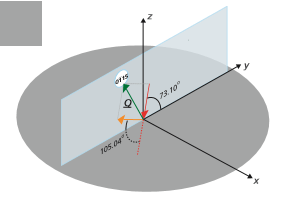
Consider the 0001 table on page 4 and the entry for the 0115 reflection. Figure 5 shows how the reflection is found. The incident beam is in the y azimuth pointing in the negative direction (-y). The angles for ω = 73.10° and 2θ = 105.04° are shown. When one reflection has been found the relevant x, -x, y, or -y azimuth can be identified on the sample and the other orthogonal azimuths can be found at positions with Φ = +90°, +180° and -90°.
Figure 5. Diagram illustrating the angles required for the 0115 reflection for the 0001 polar orientation in coplanar geometry
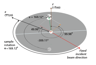
Consider the 1100 table on page 7 and the entry for the 1124 reflection. Figures 6 and 7 show how the reflection is found. Figure 6 shows the positions that the incident beam and the detector must take in order to measure the in-plane 1124 reflection.
For the in-plane configuration on the MRD (XL), a known Φ position on the sample needs to be calibrated. Figure 7 shows the total sample rotation (Φ = 169.12°) that would be required to measure the 1124 reflection assuming that the incident beam direction is fixed and initially parallel to +x. Note that to use the sample rotation value, Φ (= -90-ω-) in the in-plane tables, it is necessary to calibrate the sample Φ position by finding a reflectionand setting the Φ position to the corresponding tabulated Φ value in Data Collector: sample offsets [4].
Figure 6. Diagram illustrating the angles required for the 1124 in-plane reflection for the 1100 non-polar orientation
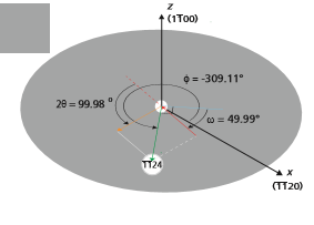
Figure 7. illustrating the sample rotation required for the 1124 in-plane reflection for the 1100 non-polar orientation
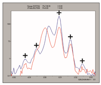
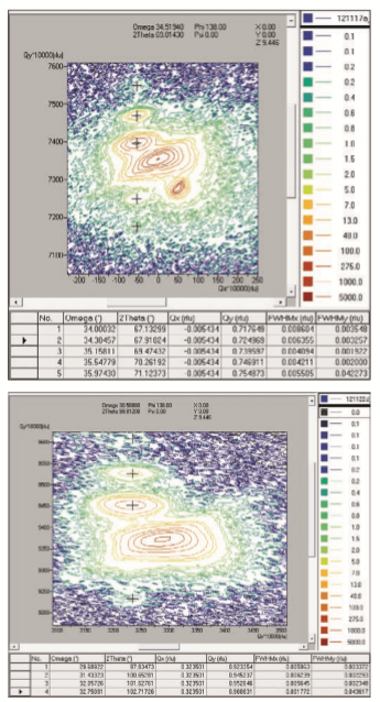
The data shown here have been obtained on an X’Pert PRO MRD using a mirror, monochromator and triple bounce analyzer. The sample was a MQW on a 2112 oriented GaN buffer layer [5]. The upper right hand image shows a high- resolution reciprocal space map (RSM) measured around the 2112 symmetric peak. The lower right hand image shows a similar RSM measured around the 2114 asymmetric peak. In both cases satellites from the MQW are clearly revealed (indicated by the crosses). Vertical scans extracted from the maps to include the crossed positions are shown above. The blue data are obtained from the 2112 symmetric peak and the red data from the 2114 asymmetric peak. Data such as this allows for more detailed analysis of MQW layer thicknesses and crystallographic quality [6].